Mini Electronic Piano with 555 Timer
It lets you play the seven basic notes, each corresponding to a button, with a basic circuit built around the ever-present 555.
Building your first musical instrument is something many electronics experimenters value, whether for their own enjoyment or to let young children play. A few components, perhaps a dedicated or general-purpose integrated circuit, can bring great satisfaction and let you play well enough to take your first steps among notes and scores.
One example is the 555, a very popular IC of which we propose here one of its many surprising transformations. It demonstrates once again how this timeless integrated circuit is probably the most versatile.
We will see how to place it in a simple network of resistors and capacitors, equipping it with a loudspeaker and seven normally open pushbuttons. In this way it becomes a basic electronic keyboard, whether piano or organ, with which to play your first melodies.
The project is aimed at everyone, including beginners: we designed it with traditional components, to be mounted on a common single-sided printed circuit board. Let us see how it was made, analyzing the circuit schematic.
How the 555 works in astable configuration
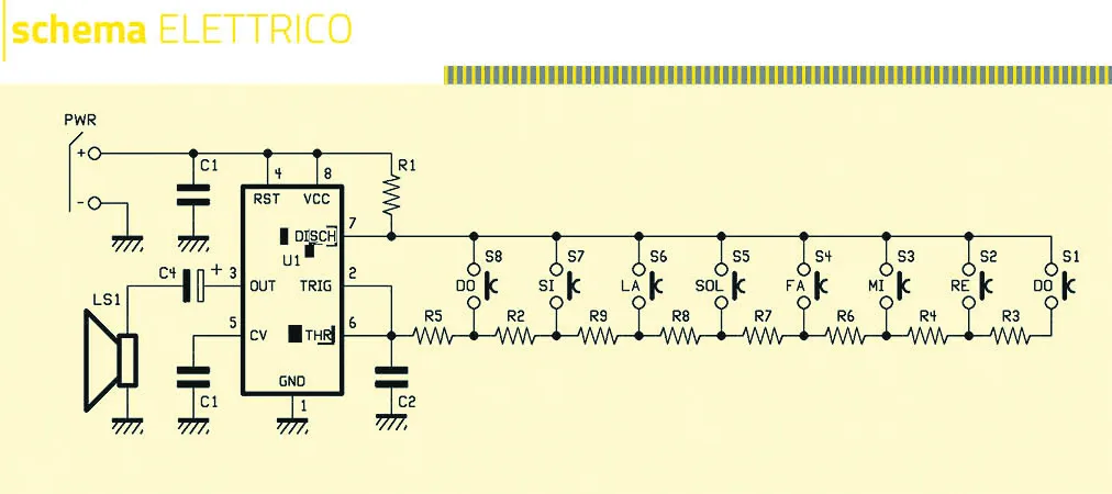
We find the ever-present and versatile 555 in a canonical configuration, that of an astable multivibrator. Although the timing network is dotted with pushbuttons and seemingly extra resistors, and the output drives a moving-coil loudspeaker decoupled by an electrolytic capacitor, the IC works exactly as an astable multivibrator according to the conventional schematic.
To understand it, let us first look at how the 555 is made and how to make it work in astable mode, with the output (pin 3) cyclically switching its logic state. The internal block diagram in Fig. 1 shows two comparators with a voltage reference obtained from a divider made of three resistors. The upper one has its non-inverting input connected to the Threshold pin (THR, pin 6), while the lower one has its inverting input brought out through pin 2 (TRIG), which acts as the trigger.
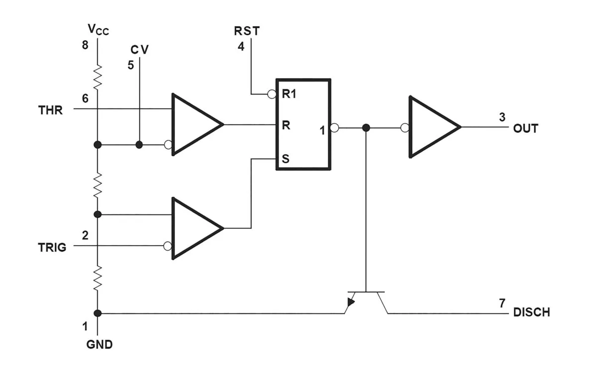
The voltage divider provides the reference for the upper op-amp at its inverting input and for the lower one at its non-inverting input. The node between the first and second resistor of the divider (powered, like the other internal stages, from pin 8) is brought out through pin 5 (CV, Control Voltage). This allows you to alter the comparator reference voltages and therefore control with an external voltage the working frequency in astable configuration, or the pulse duration in monostable timer mode.
In astable configuration, lowering the voltage on pin 5 shortens the output switching period and increases the generated frequency. Conversely, letting the voltage rise to its characteristic level (open-circuit) or increasing it lengthens the period and reduces the frequency. For the purposes of this project we do not need to manage pin 5, although it would be possible to add a “pitch” potentiometer to vary the tone of the notes during play.
Since we are not using pin 5, we filter the corresponding divider with capacitor C1, for more stable 555 operation and notes at a constant frequency. The outputs of the internal comparators go one to the RESET (upper comparator) and one to the SET (lower comparator) of an RS flip-flop. Its direct output (Q) goes high when SET is high, or to logic zero if SET is at about zero volts; the RESET output behaves in the opposite way.
The flip-flop also has a complemented output (/Q), inverse of Q; in the 555 it is connected, through a resistor, to the base of an NPN transistor configured as open collector, with the emitter at ground and the collector at the DISCH pin (Discharge, 7). The direct output Q is instead connected to the OUT pin (3) through an internal push-pull buffer, capable of sourcing up to 200 mA — enough to drive the small loudspeaker in our application.
The negative supply, that is the reference ground of the 555, corresponds to pin 1, while pin 4 (RST) is connected to the flip-flop reset, which allows you to forcibly reset the circuit by applying a low logic level from outside. In the circuit, the 555 is configured as astable: we find a resistor between pins 4, 8 and 7, one between 7 and 2, 6, and a capacitor between the latter and ground.
The resistor inserted between pins 4, 8 and 7 (which we call Ra) can be chosen by the pressed button, among S1 to S8, which allow you to play the notes of one octave plus a high C: respectively C, D, E, F, G, A, B, high C. The chosen octave is the one to the right of the middle octave of a classic 88-key piano keyboard. To simplify the circuit we did not include semitones, that is the “black” keys of the piano.
The charge and discharge cycle that generates the sound
To understand how the circuit produces sounds, let us analyze the 555 operation imagining that at power-on all capacitors are discharged. Ignoring C2, which charges almost immediately without significantly altering the comparator activity, the initial condition sees pins 2 and 6 at about zero volts and the lower comparator output at a high level. This sets a high logic level on the SET input of the flip-flop and on output Q, while /Q goes to logic zero, leaving the transistor connected to DISCH off and the capacitor free to charge.
At this point C2 begins to charge through the current flowing in the series R1-Ra (the resistance inserted by the buttons), until the voltage across its plates exceeds the threshold of the lower comparator, equal to 1/3 of the voltage applied to pin 8. At that point the comparator output goes to logic zero and releases the SET of the flip-flop, whose output nevertheless stays high until the voltage on C2 exceeds 2/3 of the supply voltage, the switching threshold of the upper comparator.
When this happens, the upper comparator output goes high and resets the flip-flop: the direct output goes to logic zero, while /Q goes high and saturates the transistor connected to pin 7, which discharges C2 through Ra. This situation remains until the voltage on C2 drops below the switching threshold of the lower comparator: at that point the output returns high and sets the flip-flop again, bringing Q back to logic 1 and /Q to zero.
The capacitor then starts charging again, because pin 7 returns to behaving like an open circuit, until it again reaches 2/3 of the voltage between pins 1 and 8: the cycle restarts. As a result of this behavior, the OUT output stays high for the time it takes C2, while charging, to go from 1/3 to 2/3 of the supply voltage, and low for the time in which C2, while discharging, goes from 2/3 to 1/3.
The times depend on the values of R1 and the resistance inserted between pin 7 and pins 2, 6 according to the pressed button; from these varies the frequency generated by U1, which is:
f = 1.44 / C2 (R1 + 2Ra)
Calculating the frequency of the notes
From the schematic we note that Ra depends on the total resistance inserted by the buttons: it can be only R5 if S8 is pressed, or the sum of R2, R3, R4, R5, R6, R7, R8 and R9 if S1 is pressed. The circuit is in fact designed with a resistor ladder that can be bypassed by the buttons, as an alternative to the more immediate solution with many resistors in parallel, one per button.
This technique allows, if multiple buttons are pressed together, to always play only the note with the highest frequency among those corresponding. For example, pressing S8 and S5 together, the circuit plays the note of S8, because that button short-circuits the rest of the timing network to its left. With the parallel-branch solution, instead, pressing multiple keys would produce intermediate notes from the parallel of the resistors: our solution ensures that the instrument is perfectly monophonic.
Pressing button S8 plays the highest note, the high C, whose frequency — considering Ra=R5 — is equal to:
f = 1.44 / 0.1µF (1 kΩ + 2×10 kΩ) = 685.7 Hz
Pressing instead S1 inserts all the resistors, whose sum (Ra) is 23 kΩ: this gives the lowest frequency, corresponding to the initial C of the octave:
f = 1.44 / 0.1 µF (1kΩ + 2×23 kΩ) = 306.4 Hz
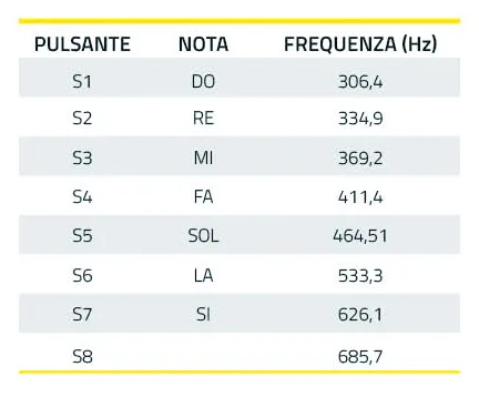
The other buttons step through intermediate values, theoretically each at 1/8 of the distance between the two C notes, because the distance between the same note in adjacent octaves corresponds to double the frequency. We had to adjust the frequencies slightly to match the resistor values available in the E24 series, arriving at the values shown in Table 1, with the frequency of each note.
From waveform to duty-cycle
The waveform generated by the 555 is practically square, at least for the notes where the resistance inserted between pins 7 and 2-6 is clearly higher than R1. The pulses become wider relative to the pauses as the pressed button gets closer to S8, because the pulse duration is:
th = 0.693 (R1+Ra) C2
while the pause lasts:
tl = 0.693 x Ra x C2
and coincides with the phase in which the DISCH pin discharges capacitor C2. The duty-cycle (dc) of a rectangular wave equals the ratio between pulse and period:
dc = th / T
Since the period T is the sum of th and tl, and th depends on the sum of R1 and Ra, the larger the latter, the closer the duty-cycle gets to 50%.
Now that we understand how the 555 works, the signal from the OUT pin feeds the moving coil of speaker LS1, coupled through the electrolytic capacitor C4 placed in series. C4 is not so much needed to block the DC component — the astable 555 never has a constantly high output — but rather to simulate an alternating waveform across the speaker.
When OUT is high, current flows into the capacitor toward the coil of LS1; when OUT switches to zero, the capacitor discharges through the speaker, generating a reverse current flow. The alternating current has exponential rise and fall edges, due to the charging and discharging of C4, which dampens the harmonics that could alter the timbre of the notes with a pure square wave. Power is applied to the + and – PWR terminals and reaches the power pins of the 555, filtered by ceramic capacitor C1 to eliminate any noise.
Practical construction
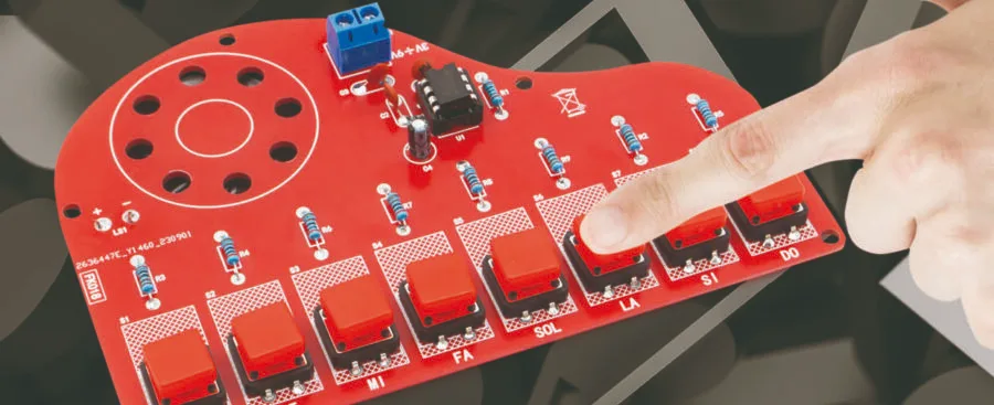
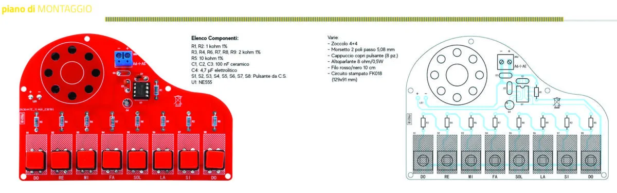
The PCB has the shape of a piano, to be obtained after etching and drilling the circuit board. It can be cut out with tin snips or a fret saw, then finishing the edge with progressively finer sandpaper.
Once the PCB is ready, arrange the few required components, all through-hole (THT) type: no SMD parts to handle. Start with the resistors and the socket for the 555, oriented as shown in the assembly plan, then move on to the buttons and capacitors, starting with the non-polarized ones and finishing with the electrolytic C4, which has a polarity to respect.
Finally, mount the two-pole screw terminal with 5 mm pitch and insert the 555 into its socket, aligning the reference mark on the top of the body with the notch of the socket, checking that no pin bends under the body during the operation. Using a short piece of small-diameter red-black wire, connect the + and – LS1 output contacts to the speaker terminals, respecting polarity; secure the speaker to the bottom of the PCB with silicone sealant or hot glue, making sure it does not touch the traces.
At this point the circuit is ready: it requires no calibration or preliminary steps. You can start playing right away.